The LBE-1423 Differential GPSDO locked clock source outputs a high purity signal frequency locked to GPS. It offers a stable low jitter differential clock for FPGA inputs with lower phase noise than the LBE-1420 and 1421.
Frequency stability is defined by accurate GNSS satellite (cesium-based) references and approaches 1.0E-12 or 0.000001 ppm. Output phase noise is shaped by an internal TCXO to provide a clean clock signal with sub-picosecond RMS jitter. Multi-loop digital-analog PLL allows output frequency to be set to any value between 1 Hz and 1.4 GHz with finite resolution (e.g., 144,800,000.025 Hz.
The differential output signal is a 3.3V CMOS square wave with 50O source impedance. It can be used as a differential clock source for various devices.
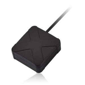
Includes a magnetic base active GPS antenna.
Output power level (at 10MHz, fundamental power channel): +11dBm. Typical phase noise at 10MHz:
-72 dBc/Hz at 1 Hz
-101 dBc/Hz at 10 Hz
-128 dBc/Hz at 100 Hz
-147 dBc/Hz at 1 kHz
-156 dBc/Hz at 10 kHz
-159 dBc/Hz at 100 kHz
-164 dBc/Hz at 1 MHz
Power draw through 5V USB is 250mA. Rise/fall time of output signal at 10MHz is 300ps/260ps measured between 10% and 90% levels.
Specifications:
- 69mm x 40mm x 12mm (including connectors)
- USB-C Connector 5V 250mA max
- GPS SMA provides 3.3V 30mA max
- Output 1 SMA 1 PPS Square Wave
- Output 2+/- SMA 1Hz-1.4GHz 3.3V 50O Square Wave
- CE FCC UKCA certifications
- Two year warranty
Instead of sending a clock signal referenced to ground (single-ended), a differential output sends two opposite signals. One carries the clock, the other carries its inverted version. The receiver looks at the difference between the two. This approach provides better noise rejection with cleaner signal edges and lower jitter.


